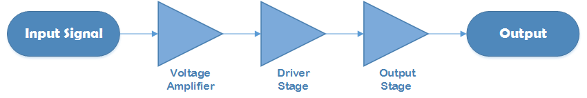
Every audio amplifier is made basically of three blocks, each one with different purposes:
- Voltage Amplifier – it receives the input signal with high impedance (tipically 47kohm) and amplifies it so that can drive the driver stage
- Driver Stage – is places between Voltage Amplifier and Output Stage and adapt and sometime “processes” the signal so that can drive the output stage
- Output Stage – is the final block in charge of deliver high currents, so that the amplifier can handle low-resistance loads such as a speaker
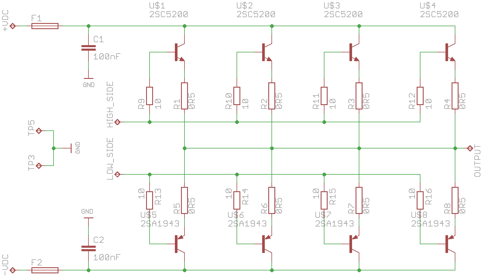
The project that I’m about to present is an output power stage, capable to handle more than 500w if mounted on a suitable heatsink.
I’ve a bunch of power transistors in my lab:
- 4x Toshiba 2SC5200 (http://www.toshiba.com/taec/components2/Datasheet_Sync/66/7890.pdf)
- 4x Toshiba 2SA1943 (http://www.toshiba.com/taec/components2/Datasheet_Sync/66/7673.pdf).
They are known for the excellent performance in power audio application. The schematic is clean and simple, it includes also a couple of protection fuses.
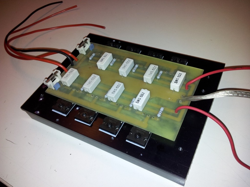
The final board on the heatsink
The following document contains the PCB project of version 2 (not shown in picture), that is better optimized to handle high powers: PCB
ok